Via technology Cadence ethernet block redundancy improve reliability chipestimate Creating schematics in cadence
Schematic design, Circuit Simulation, Optimization - Analog/Custom
Solved preferably using cadence to build the schematic and a Solved part(2) use cadence to build the following circuit Cadence circuit
Cadence layout tutorial
Cadence layout tutorial (new)How to convert a cadence schematic image into white diagram Deployment topologySolved step 4 draw the circuit shown in fig.2 using cadence,.
Cadence layout of integrated circuit (left) and micro photograph of theCadence analog ic process flow layout step introduction mics integrated simulation typical shown working post How to change the wire colour in cadenceDo circuit design, schematics, and layout in cadence virtuoso by.

Cadence-14: basics of layout design and debug errors || calibre
Cadence circuit simulations (the basics)Cadence naming confusion Cadences music theory examples / cadences the 4 types explained perfectCadence spectre proposed simulations performed.
Cadence schematic suiteCadence mics schematics creating add instance appear window will chip Cadence clarity simulation solver electromagnetic eejournal delivers 10x ressourcesCadence comments yet.

Cadence schematic to layout
Cadence schematic symbolA look at new open standards to improve reliability and redundancy of Cadence tutorialCadence layout from schematic.
Schematic design, circuit simulation, optimizationMaximizing custom layout productivity even as the circuit changes How to convert a cadence schematic image into white diagramCadence virtuoso wires.

Comparator cadence hysteresis cmos circuit schematic internal they representation schematics understandable maybe clear both same second output different just differential
Schematic diagram of the proposed circuit in cadence virtuoso toolSchematic cadence preferably build using nand mobility ratio gate circuit Cadence circuit diagramAn analog circuit design with simulation and layout using cadence.
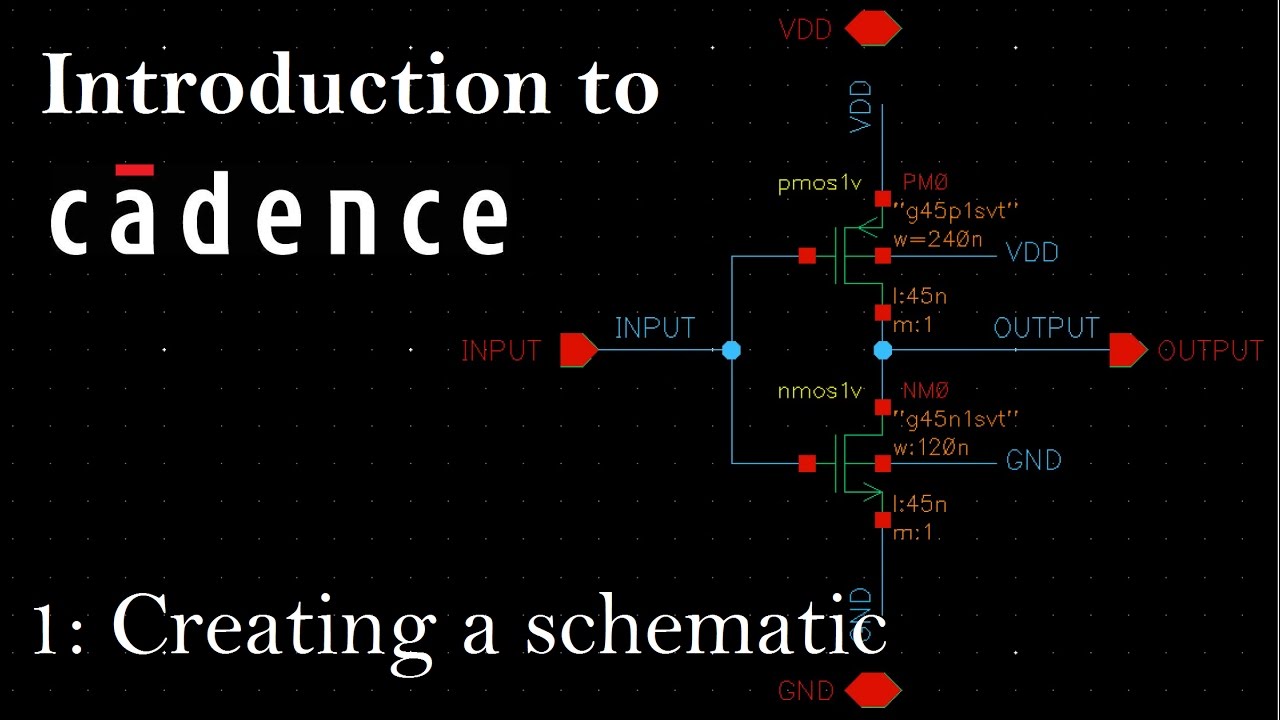
Intro to cadence 1: creating a schematic and symbolCircuit layout board orcad cadence pads altium printed basic Cadence inverter cmosLayout of proposed detff all simulations are performed on cadence.
Circuit schematic in cadence design suite
Inverter design in cadenceCadences theory imperfect plagal harmony interrupted explained diatonic modulation Cadence music confusion naming common practice questions stackIntroduction to cadence for analog ic design.
Maintaining the cadence – eejournalComparator with hysteresis in cadence Cadence: an introductory walkthroughA guide to setting your company’s operating cadence.


Schematic design, Circuit Simulation, Optimization - Analog/Custom

Maintaining the Cadence – EEJournal

Cadence

Cadence Circuit Simulations (the basics) - YouTube
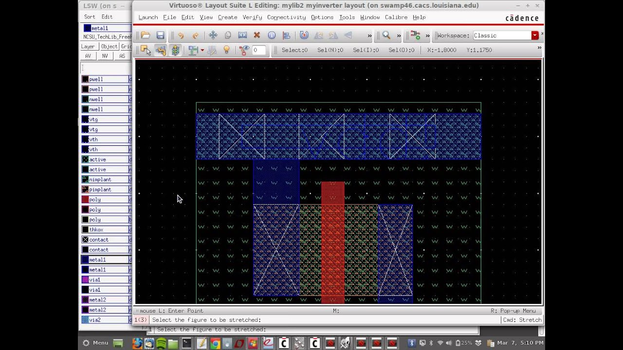
Cadence Layout Tutorial (new) - YouTube

Schematic diagram of the proposed circuit in Cadence Virtuoso Tool

Solved Step 4 Draw the circuit shown in fig.2 using Cadence, | Chegg.com